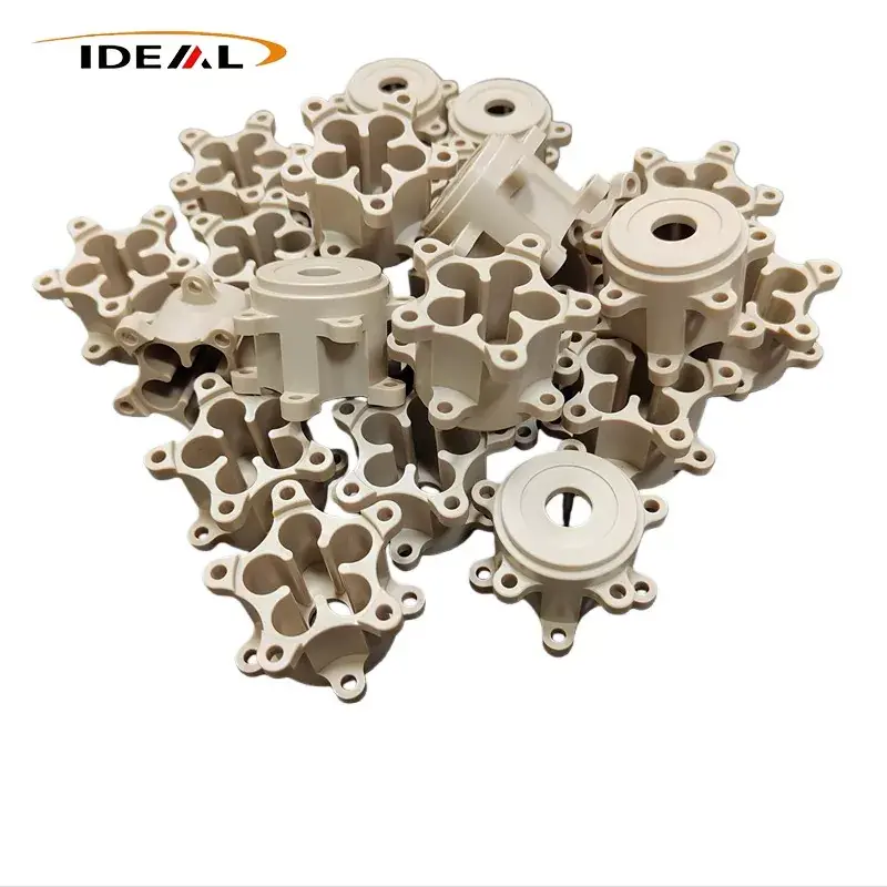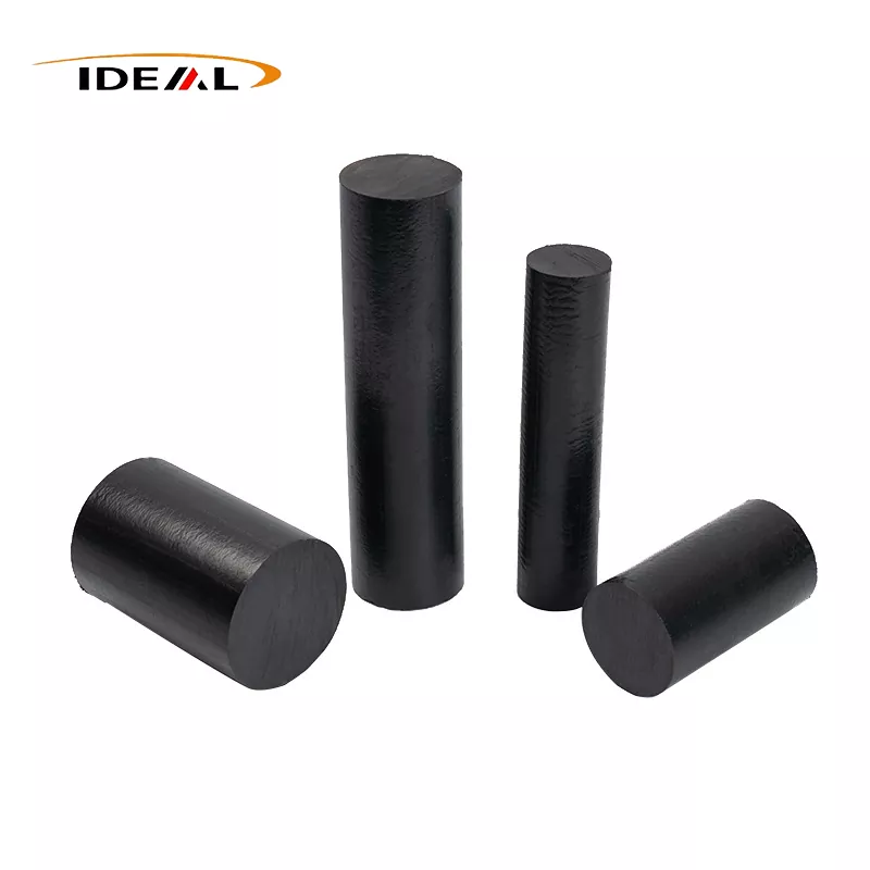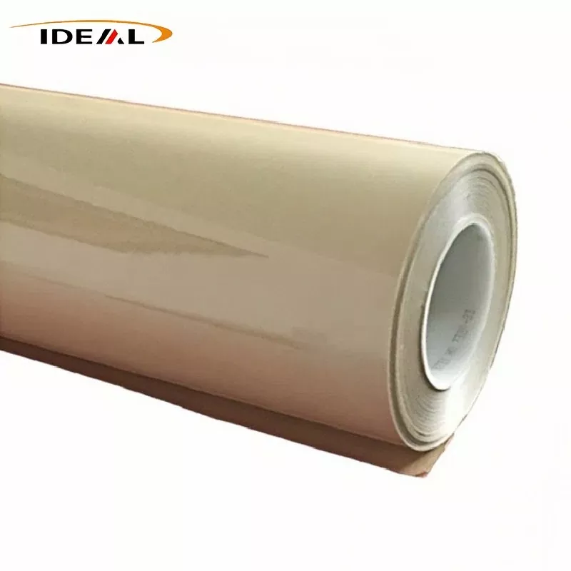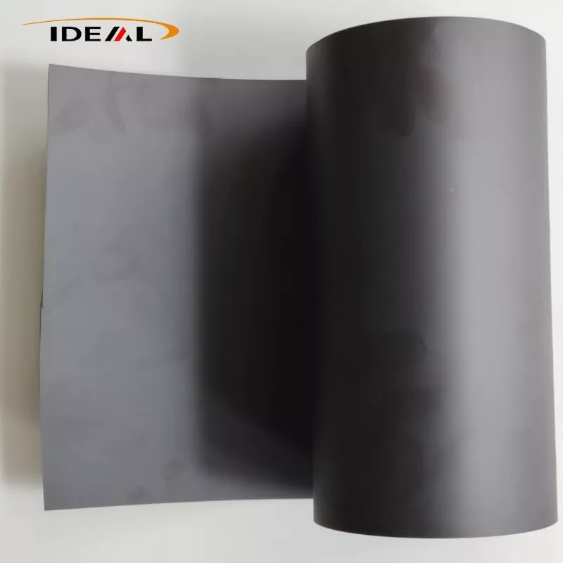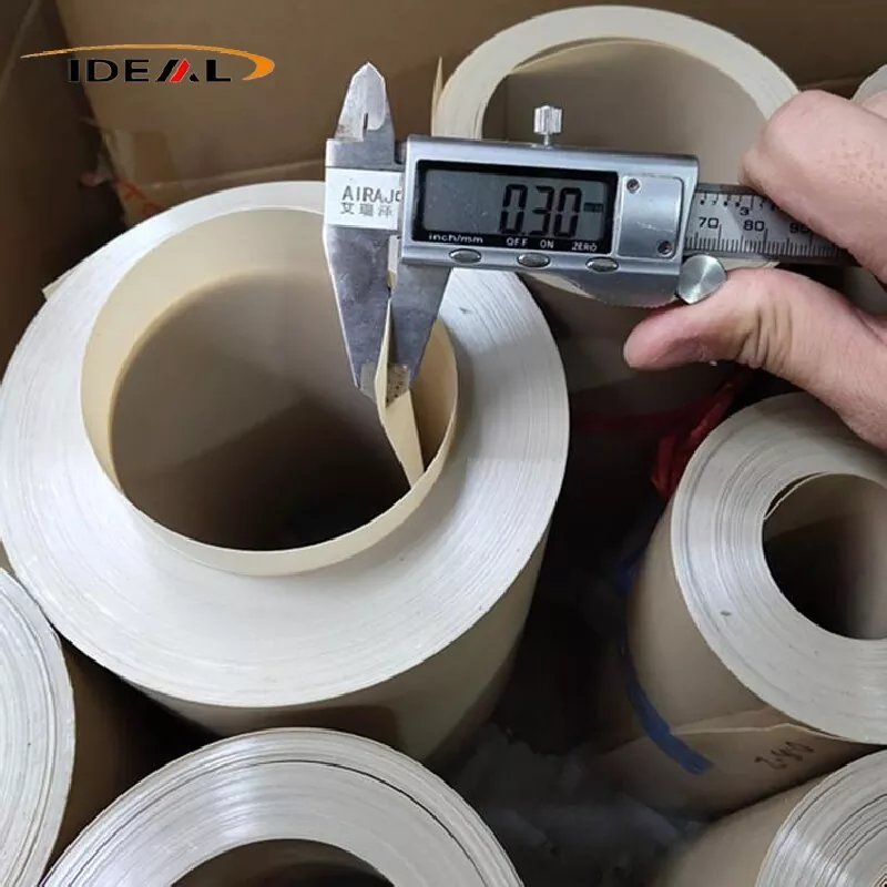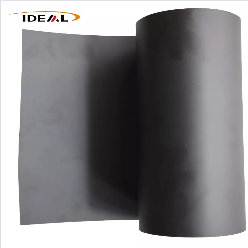
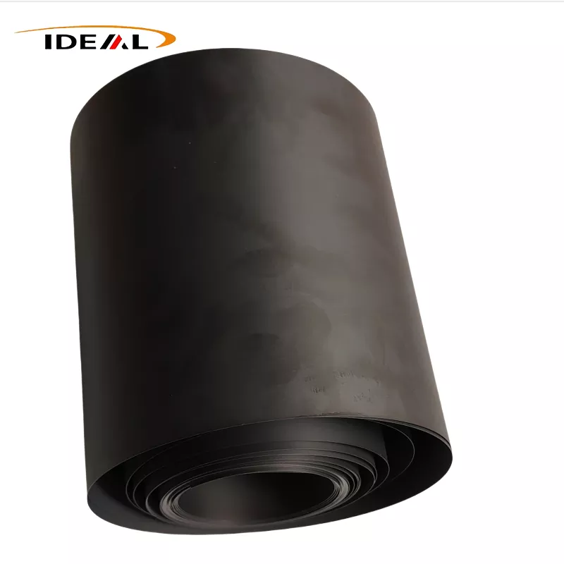
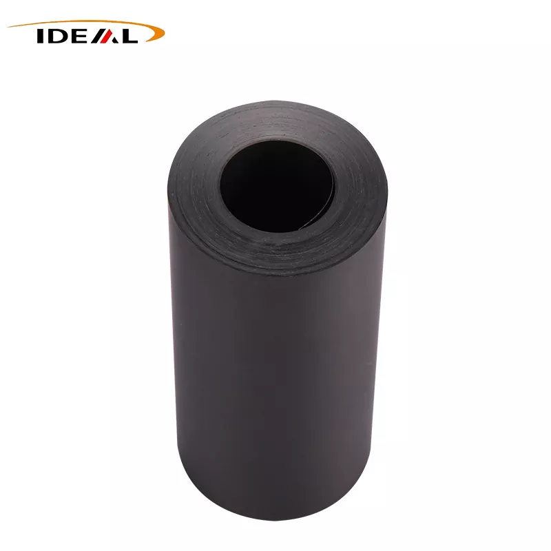
Guangzhou Ideal supply Permanent ESD PEEK Film with surface resistivity 10⁶–10⁹ Ω/sq, high temp resistance -200℃ to 260℃, low outgassing, carbon nanotube modified ESD PEEK sheet for wafer vacuum chuck, probe station, electronic fixture. Custom thickness & size available.
ESD PEEK film is internally filled and modified with carbon nanotubes or ultra-fine carbon black and manufactured via extrusion casting or mirror calendering processes. It integrates outstanding static-dissipative performance, high-temperature resistance, mechanical robustness, solvent cleaning resistance, flame retardancy and radiation resistance. It is widely applied in semiconductor manufacturing and new energy industries.
Anti-static PEEK Film differs fundamentally from conventional surface-coated static-dissipative plastic films. Surface-coated films are low-cost and transparent, yet their anti-static coating delaminates above 120°C and fails completely after solvent cleaning. Such films are only suitable for short-term low-temperature applications. In contrast, conductive fillers in ESD PEEK film are uniformly dispersed within the PEEK matrix, delivering permanent static-dissipative performance. No coating delamination or anti-static failure occurs during polishing, solvent cleaning, or long-term high-temperature service.
Guangzhou Ideal has specialized in PEEK film research and production since 2014, accumulating over 12 years of professional industry experience. Our ESD PEEK film series includes high-end carbon nanotube (CNT) semiconductor-grade types, general industrial grades filled with ultra-fine conductive carbon black, and carbon fiber-reinforced ESD grades.
1. CNT high-end semiconductor grade
Carbon nanotubes are one-dimensional tubular nanocarbon materials with an ultra-high aspect ratio. A continuous three-dimensional conductive network can be formed with extremely low filler loading. All carbon nanotubes are fully encapsulated by the resin matrix with no free carbon particles generated. This grade is ideal for high-cleanliness semiconductor precision processes including wafer handling, probe station operation, vacuum chamber systems and optical applications.
2. Ultra-fine conductive carbon black industrial grade
Consisting of spherical carbon particles that form conductive networks through inter-particle contact, this grade features a stable surface resistivity range of 10⁶–10⁹ Ω/sq with uniform resistance distribution and weak anisotropy. A relatively high filler loading is required to achieve qualified ESD performance. Excessive carbon black addition reduces film toughness and causes friction-induced carbon shedding with poor surface cleanliness. It is not applicable for high-end semiconductor wafer processes and is mainly used for ordinary electronic fixtures, lithium battery components, high-temperature tooling and general explosion-proof equipment for cost-effective mass production.
3. Chopped carbon fiber reinforced grade
PAN-based chopped carbon fiber provides both static dissipation and structural reinforcement, delivering enhanced mechanical strength and abrasion resistance. Its surface resistivity ranges from 10⁴–10⁷ Ω/sq. The main limitation is conductive anisotropy formed during extrusion casting, resulting in slight MD/TD resistivity deviation. This versatile flagship grade is widely used for semiconductor fixture liners, SMT high-temperature gaskets and lithium battery tooling.
Note: Not all carbon-filled PEEK films feature qualified ESD performance. High-filler CF30 carbon-rich PEEK exhibits excessive conductivity and cannot be used as standard static-dissipative ESD film.
With over a decade of technical accumulation, high-end production equipment investment and standardized quality control systems, Guangzhou Ideal has solved critical quality pain points in ESD PEEK film manufacturing.
1. Custom twin-screw extrusion equipment with optimized screw configurations balances uniform filler dispersion and intact fiber structure, eliminating high-temperature resistivity drift and ensuring stable surface resistivity after repeated thermal cycles.
2. By lowering traction tension and draw ratio and adopting gradient annealing treatment, we effectively mitigate conductive anisotropy and directional resistivity deviation.
3. Precision gradient annealing with strictly controlled temperature rise and cooling rates releases residual internal stress, significantly reducing warpage and curling after slitting and die-cutting.
4. Modified granulation is completed in a dust-free environment to protect fiber-matrix interfacial bonding. This solves interfacial debonding and friction-induced carbon shedding, preventing micro-particle contamination and wafer scratching.
Semiconductor-grade ESD PEEK film provides stable resistivity of 10⁶–10⁹ Ω/sq for uniform static discharge, preventing high-voltage breakdown of wafers and IC chips. Semi-insulating grades (10¹⁰–10¹² Ω/sq) balance insulation and static suppression with minimal high-temperature drift. The film supports continuous operation at 260°C with resistivity fluctuation controlled within 5%, eliminating static accumulation in vacuum environments.
ESD PEEK film offers a continuous service temperature range of -200°C to 260°C and short-term heat resistance up to 340°C. It remains crack-resistant at low temperatures and resists softening, thermal flow, deformation and warpage at high temperatures, maintaining stable dimensional performance under alternating thermal cycling.
The film features high tensile and tear strength. Ultra-thin specifications resist fracture and repeated bending cracking. With self-lubricating properties, a low friction coefficient and low wear rate, it delivers excellent long-term structural stability. Low creep deformation ensures no structural collapse for gaskets and lining films under sustained high-temperature pressure.
Anti-static PEEK Film withstands most strong acids, alkalis, ketones, esters, alcohols and industrial cleaning solvents, with only concentrated sulfuric acid capable of dissolving the PEEK substrate. Featuring ultra-low ionic leaching and minimal particle shedding, the film meets Class 1 and Class 10 ultra-clean workshop standards and avoids wafer and optical lens contamination.
1. Semiconductor wafer manufacturing
As a core material for semiconductor precision processes, ESD PEEK film’s permanent static dissipation, high-temperature stability, low outgassing and zero powder-shedding properties make it ideal for wafer vacuum chuck liners, probe station thermal-insulating ESD gaskets, and wafer carrier isolation films.
2. Precision electronics, PCB and testing fixtures
Its outstanding high-temperature resistance enables production of ESD insulating films for high-temperature functional testing fixtures, FPC high-temperature protective films, SMT thermal tooling gaskets and electronic mold insulation components.
3. Lithium battery and new energy industry
ESD insulating films prevent short circuits and fire risks caused by frictional electrification of electrode sheets. Flame-retardant, high-temperature resistant and anti-static lining films are applied to battery explosion-proof equipment to improve overall operational safety.
Cause: Absence of gradient annealing leaves locked-in residual stress inside the Anti-static PEEK Film. High-temperature processing releases residual stress and relaxes polymer chains, causing slippage and reconstruction of the internal conductive network. This results in random resistivity deviation, with local areas turning insulating or excessively conductive.
Root cause: Poor fiber-matrix interfacial bonding, rather than inherent carbon fiber fragility.
A. Excessive screw shear during granulation over-crushes carbon fibers and damages the resin encapsulation layer.
B. Residual commercial sizing agent on raw carbon fibers causes interfacial debonding after high-temperature exposure.
Solution: Remove residual fiber sizing and apply PEEK-specific modified sizing agents to strengthen fiber-matrix interfacial bonding and suppress friction-induced particle chipping.
Cause: Carbon fiber agglomeration during granulation forms surface fiber pits after casting. Overlapping fibers at agglomeration points create localized high-conductivity micro-regions with drastically low resistivity, bringing risks of local electrical ignition.
Control method: Optimize granulation parameters to balance filler dispersion and fiber length retention. Implement multi-point transverse resistivity inspection across the entire film width, instead of only testing roll head and tail sections.
1. Unqualified annealing temperature curve.
2. Excess winding tension induces residual storage stress. Although flat upon factory inspection, the film gradually warps as internal stress releases during storage.
Solution: Adopt customized low-tension winding parameters for thin-gauge films; standard parameters for 0.3–0.5mm films are not applicable.
1. We adopt internationally sourced high-purity anti-static PEEK raw materials and combine them with mature proprietary manufacturing technology. Our ESD PEEK film avoid local defects caused by carbon particle agglomeration, including localized low-resistance zones and insulating dead spots. Poor filler dispersion easily triggers local electrostatic breakdown and short circuits at customer workstations, resulting in batch scrapping and substantial economic losses.
2. Our ESD PEEK films feature high dimensional accuracy and ultra-low internal stress, resisting warpage and shrinkage under high-temperature cycling. With uniform static-dissipative dispersion and zero particle diffraction, the material prevents black micro-particle detachment in high-temperature vacuum environments, effectively avoiding wafer and optical lens contamination and yield reduction risks.
3. Resistivity difference between the machine direction and transverse direction on the same film roll is minimal. The overall resistivity deviation within a single roll and between different batches is strictly controlled within one order of magnitude.
4. We provide customized resistivity grades, Film thicknesses and slitting sizes for global semiconductor, precision electronics and aerospace clients. Customers may submit product drawings, operating temperature parameters and surface resistivity requirements. Our engineering team will deliver a complete material performance report and factory-direct quotation within 24 hours.
A1. Pure unfilled PEEK delivers excellent insulating performance with surface resistivity up to 10¹⁴ Ω/sq. It easily accumulates static charge, which can damage ultra-precision components such as wafers and IC chips. ESD-modified PEEK film effectively dissipates static electricity while fully retaining all superior mechanical, thermal and chemical properties of pure PEEK resin.
A2. No. Particle shedding originates from weak bonding at the carbon fiber and resin matrix interface, which is formed during upstream formulation and granulation. Subsequent polishing and cleaning can only remove surface floating carbon powder, but cannot repair internal interfacial defects. Friction will still cause particle shedding after long-term use.
A3. High-quality carbon fiber-filled ESD PEEK forms a stable internal conductive network with no aging or performance decay. Unlike surface-coated anti-static films, its static-dissipative properties are permanent. However, if the fiber-matrix interface is damaged, continuous friction-induced debris accumulation will alter local ESD performance.
A4. Carbon fiber-filled ESD PEEK exhibits inherent conductive anisotropy caused by fiber flow orientation during extrusion. Testing only one direction cannot detect abnormal internal performance. Finished product inspection must include both machine direction (MD) and transverse direction (TD) resistivity testing to control anisotropy and avoid batch quality inconsistencies for customers.
A5. During casting molding, carbon fibers align along the material flow direction, creating natural conductive anisotropy. Industry-qualified tolerance allows a resistivity difference of up to one order of magnitude between flow and transverse directions. A deviation exceeding two orders of magnitude is regarded as unqualified. Therefore, both directional resistivities must be tested during incoming inspection.
A6. By industry standard, PEEK material with thickness ≤ 0.5mm is defined as ESD PEEK film, generally produced and supplied in continuous roll form. Material with thickness > 0.5mm is classified as ESD PEEK sheet, manufactured via solid plate molding. The two categories adopt different forming and production processes.