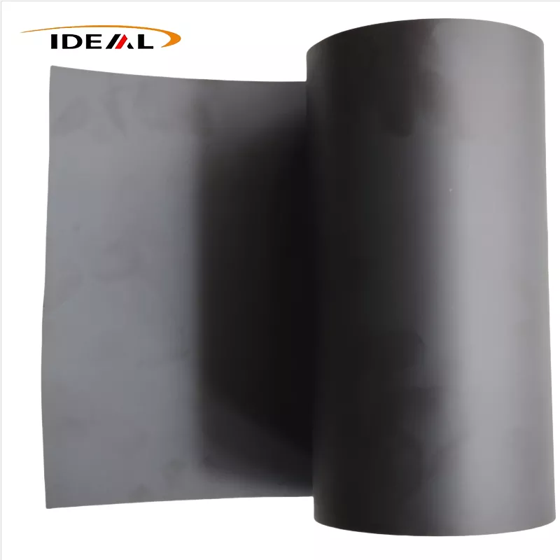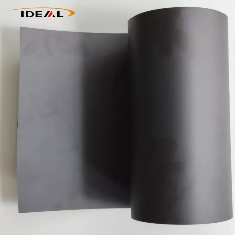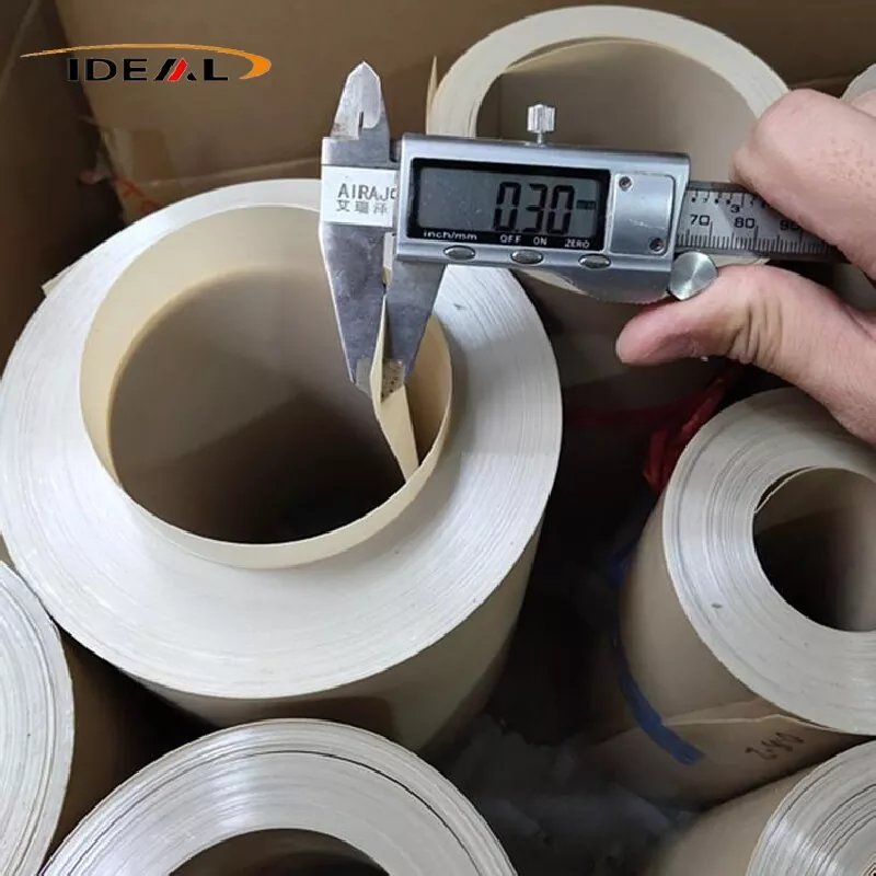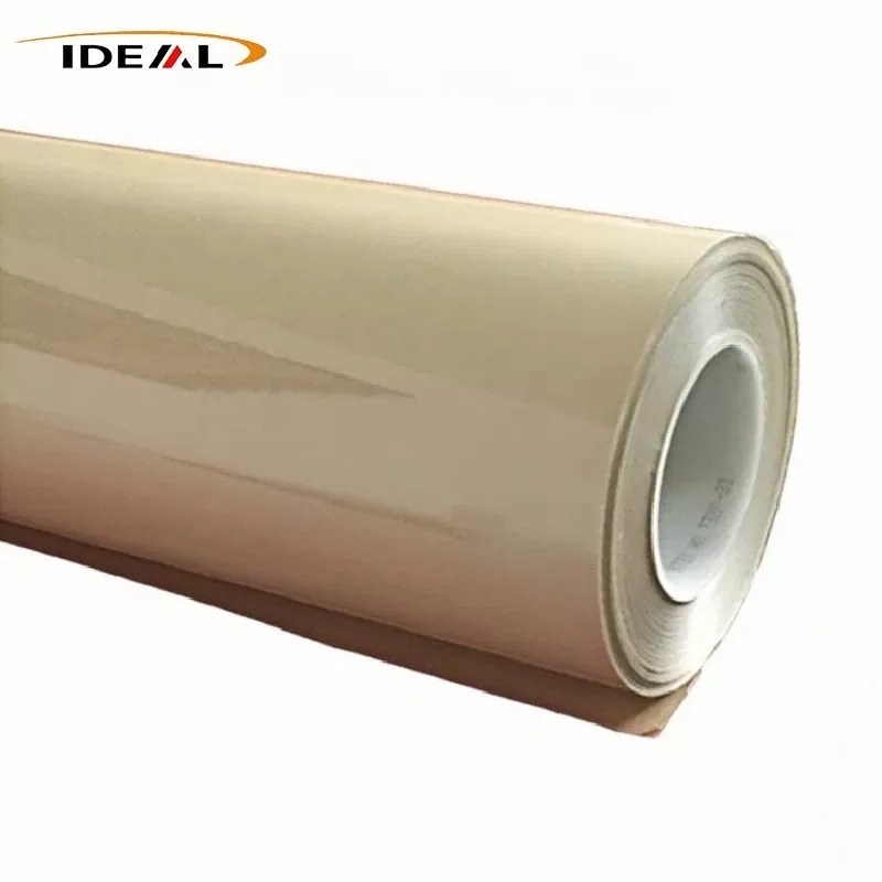
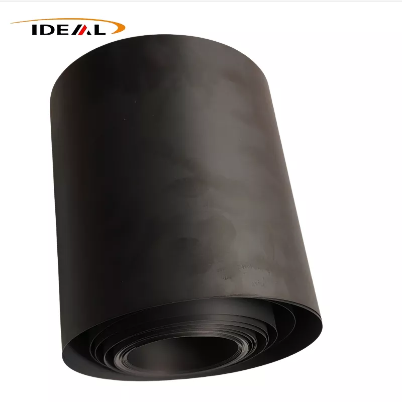
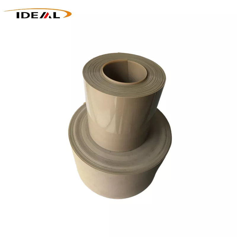
PEEK film is ultra-thin high-performance engineering plastic film extruded from virgin PEEK resin via high-temperature casting & biaxial stretching technology, split into crystalline natural beige film and transparent amorphous film as mainstream grades. Compared with PI, PET and Kapton film, it keeps stable mechanical, electrical and chemical performance under continuous 250℃ working temperature.
PEEK film is a semi-crystalline high-performance engineering plastic film. It delivers five core performance characteristics under high-temperature, strongly corrosive, high-pressure and precision operating conditions: electrical insulation, ESD protection, structural support, anti-wear sliding performance, and barrier sealing. Conventional PET, PI and PTFE films cannot meet this comprehensive set of performance requirements simultaneously.
The most widely adopted manufacturing process for PEEK plastic film is T-die melt casting. Dried PEEK resin pellets are fed into a high-temperature single-screw extruder. The molten polymer is extruded through a T-die to form a continuous film preform. The molten material is uniformly spread into a consistent film web, which is fixed and cooled by temperature-controlled calendaring rollers. The roller traction speed is precisely synchronized with the extrusion output. Online beta-ray thickness gauging enables real-time die lip adjustment, maintaining film thickness tolerance within ±3 μm. The film then undergoes professional annealing treatment. As the mainstream production technology, this process produces films with thickness ranging from 0.0125 mm to 1.0 mm, covering full-range grades including pure PEEK, ESD anti-static PEEK, and GF/CF modified PEEK.
Another mature manufacturing method is biaxial stretching. A thick cast preform is produced first and then processed in a preheated oven at 150–160°C. The preform is stretched longitudinally and transversely at precise ratios, followed by heat setting, cooling and rolling. This method produces ultra-thin, high-strength PEEK foil film with a typical thickness range of 0.005 mm to 0.15 mm.
As a high-end specialty engineering film, PEEK film faces multiple technical challenges during production and practical application.
1.PEEK features an extremely narrow processing window. With a melting point of approximately 343°C, PEEK allows very limited tolerance for extrusion temperature deviation. Slight temperature fluctuations easily cause crystalline spots, bubbles and thickness inconsistency. Carbon-filled PEEK grades exhibit poor melt fluidity and are prone to pigment agglomeration and surface pitting defects.
2.Ultra-thin PEEK film (below 0.05 mm) presents significant thickness control difficulties. Stretch forming may cause longitudinal waviness and uneven thickness. In carbon-filled films, inconsistent filler dispersion leads to unstable surface resistivity and fluctuating ESD performance.
3.Crystallinity control is technically complex and directly determines film toughness and dimensional stability. Excessively high crystallinity makes the film brittle and crack-prone, while insufficient crystallinity results in post-shrinkage deformation under continuous high-temperature conditions.
4.Surface defect control is extremely strict. Pinholes, scratches, black spots and foreign impurities are strictly prohibited. Pinholes in pure insulating PEEK film completely compromise insulation performance. Black spots in carbon-filled films indicate filler agglomeration, which causes ESD failure.
5.PEEK’s high rigidity and low friction coefficient bring challenges to slitting and conversion processes. Slitting easily produces burrs and edge warping. Friction generated during carbon-film slitting accumulates static electricity, increasing the risk of surface contamination.
6.Batch-to-batch consistency is difficult to stabilize. Minor differences in resin batches and pigment dispersion uniformity affect mechanical properties and resistivity performance, failing to meet the ultra-high stability requirements of semiconductor customers.
1.Conventional PET and PI films suffer from thermal creep and warpage under high temperatures, causing failure of FPC substrates and insulating gaskets during thermal processing.
2.Most alternative films exhibit poor chemical resistance and hydrolysis resistance, aging and cracking rapidly under strong solvent cleaning and high-temperature steam sterilization environments.
3.Long-term high-temperature and high-pressure operation leads to dielectric attenuation in ultra-thin films, increasing risks of electrical leakage and dielectric breakdown.
4.Repeated EtO and high-temperature sterilization gradually embrittles the film, resulting in cracking in long-term medical applications.
1.Temperature-induced resistivity drift is the most critical customer pain point. Low-cost carbon-filled films show dramatic resistance fluctuations after heating, leading to unstable electrostatic protection and potential damage to wafers and precision chips.
2.Poorly formulated carbon-filled films suffer from pigment precipitation and powder shedding, contaminating wafers and optical components and reducing customer production yield.
3.Repeated frictional wear shortens the service life of fixture lining films, causing rapid attenuation of ESD performance.
4.Combined high-temperature and chemical corrosion accelerates the aging of ordinary anti-static films, leading to permanent loss of anti-static functions in high-temperature cleaning environments.
PEEK foil is widely used in high-precision fields including semiconductors, flexible printed circuits (FPC), and medical devices. Minor defects such as pinholes, thickness variation, residual internal stress, surface particles, and ionic leaching can cause full-batch rejection in customers’ production processes. With over twelve years of professional manufacturing experience, Guangzhou Ideal adopts mature T-die melt casting molding technology and boasts standardized production workflows. Our company implements a full set of rigorous quality control systems to guarantee stable and reliable product quality.
A. Verify the official Certificate of Analysis (COA), covering melt flow rate (MFR), ash content, moisture content, residual monomer content, and metallic impurity levels.
A. Constant-temperature dehumidification and drying: Moisture content is strictly controlled and monitored in real time to eliminate extrusion-induced bubbles and pinholes.
B. Multi-stage melt filtration: A 400/800/1200-mesh multi-layer filter mesh system traps gels, carbon agglomerates and foreign contaminants to prevent black spots and crystalline point defects.
A. Closed-loop control of melt temperature and pressure.
B. Beta ray and infrared online thickness measurement.
C. MD/TD bidirectional tension closed-loop control.
D. CCD machine vision online surface inspection.
E. Online crystallinity adjustment and cooling roller temperature zoning control.
F. Continuous online annealing process monitoring.
A. Basic physical performance testing.
B. Electrical performance testing.
C. Special high-purity testing for semiconductor-grade applications.
D. Offline re-inspection for surface appearance defects.
A. Dust-free workshop environment control.
B. Precision slitting dimensional control.
C. Strict coil end face inspection.
D. Process control for die cutting and laser processing.
E. Surface modification control via plasma and corona treatment.
Packaging, Traceability and Warehousing Control
Supported by mature production procedures and stringent full-process quality management, our products fully meet customers’ high-standard quality requirements.
A. Free of pinholes, bubbles, crystalline points, scratches, black spots, impurities, wrinkles and surface pits.
B. The film surface is clean and dust-free. Clean-grade products fully comply with dust-free workshop packaging standards.
C. Slitting edges are smooth without burrs, gaps or warpage.
A. Thickness tolerance: Film thickness variation is strictly controlled. Ultra-thin PEEK films demand ultra-high thickness uniformity.
B. Width tolerance: Stable slit width adapts to customers’ continuous coil processing.
C. Straightness: Coils feature flat geometry without waviness or warpage, ensuring smooth and deviation-free unwinding.
A. Mechanical properties: Tensile strength, elongation at break and modulus remain stable with minimal intra-batch difference. The film possesses proper toughness and effectively resists bending cracks.
B. Thermal properties: Adjustable crystallinity and low thermal shrinkage deliver outstanding dimensional stability under high temperatures and resist creep deformation.
C. Electrical properties: Natural PEEK film provides high dielectric strength and stable insulation performance. Carbon-filled ESD film maintains steady surface resistivity within the target ESD range, with minimal temperature drift and excellent inter-batch consistency.
D. Chemical resistance: The material withstands organic solvents, acids, alkalis and hydrolysis, suitable for repeated cleaning and high-temperature sterilization scenarios.
Variations in appearance, thickness, mechanical properties and resistivity within and across batches are strictly controlled within customer-specified tolerance ranges. Semiconductor clients impose particularly strict requirements on batch stability.
A. Clean-grade products: Produced and slit in dust-free environments and packed with ultra-clean bags to ensure ultra-low particulate contamination.
B. Standard-grade products: Adopts moisture-proof and dust-proof packaging to avoid surface scratches and contamination during transportation.
C. Complete marking: Grade, thickness, width, batch number and production date are clearly labeled for full product traceability.
Semiconductor-grade PEEK films require advanced control over ionic leaching, low outgassing and low particulate release.
A. Ionic contamination control: Metal and anion residues including Na⁺, K⁺, Fe, Ca and Cl⁻ are extracted via ultrapure water and controlled at the ppb level, preventing circuit leakage caused by ionic migration during wet processing.
B. Vacuum outgassing performance: Total Mass Loss (TML) < 0.5%; Condensable Volatile Condensable Materials (CVCM) < 0.1%. The material is applicable to vacuum chambers and optical components and will not produce condensed volatile residues to contaminate wafers or lenses at high temperatures.
C. Particle release control: After ultrasonic cleaning, particles ≥0.5μm are controlled below 100 pcs/cm². For carbon-filled ESD grades, we prioritize the control of friction-induced carbon shedding and filler delamination, rather than relying solely on surface resistivity testing.
D. Ash content: Controlled within 20–50 ppm. The raw materials are free of inorganic impurities and do not incorporate external lubricating additives, avoiding high-temperature precipitation commonly seen in conventional industrial PEEK materials with processing aids.
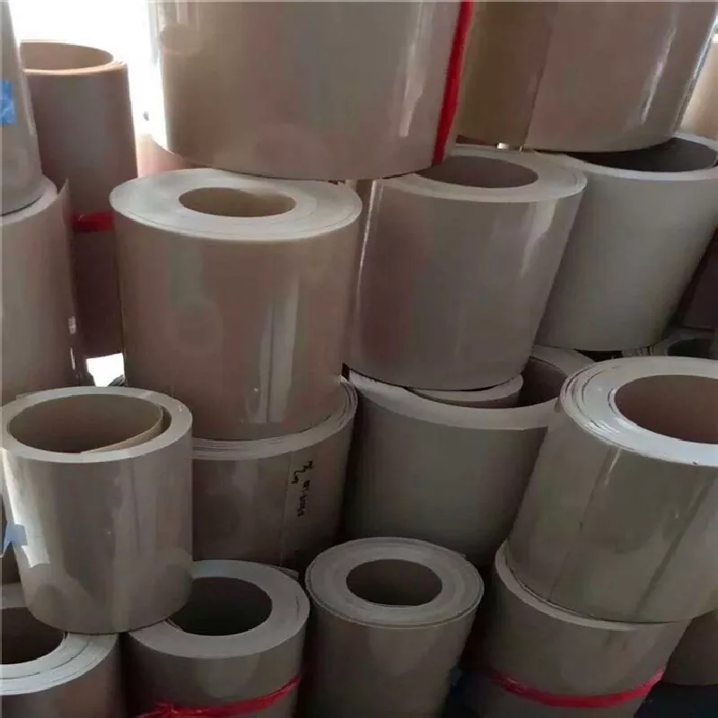
| Product name | Polyetheretherketone Film |
| Material | Pure PEEK, CF/GF filled PEEK, ESD Antistatic PEEK etc. |
| Color (Crystallinity) | light amber highly transparent, beige translucent, dark brown opaque |
| Color (filler) | black, off-white |
| Crystallinity | amorphous pure PEEK, semi-crystalline pure PEEK, fully crystalline pure PEEK |
| Conventional thickness (μm) | 25, 30, 38, 50, 75, 100, 125, 150, 200, 250, 300, 400, 500, 600, 750 (1μm=0.001mm) |
| Width (mm) | 650, 700, 800, 1000, 1250, 1450 |
| Roll length | 0.02-0.05mm: 1000–2000 m / roll;>0.05mm: 300–1000 m / roll |
| Thickness accuracy | Conventional industrial grade: thickness tolerance ±5%~±10%;High precision/semiconductor grade: ±3%~±5% |
| Width accuracy | Conventional slitting: ±0.5 ~ ±1 mm;Precision narrow slitting (for FPC, tiny gaskets): ±0.1~±0.3 mm |
| sample | To be negotiated |
| Certificates | ISO9001:2012 |
PEEK film performance varies significantly depending on its crystallinity and filler composition, which further differentiates its application scenarios.
The optimal crystallinity window for PEEK film is 28%–34%, requiring uniform crystallization across the film cross-section. A dual structure with a highly crystalline surface and low-crystallinity inner layer is unacceptable, as delamination and warpage will occur under thermal cycling. This stable structure is achieved through inline gradient cooling and continuous online annealing, rather than simple static oven baking.
1. Amorphous film: Supports thermoforming, heat sealing, and crack-free bending at room temperature. Suitable for FPC hot-press substrates, thermoformed insulating components, and high-temperature resistant optical gaskets.
2. Low-crystallinity film (crystallinity <25%): Delivers excellent toughness and thermoformability, yet exhibits high thermal shrinkage and poor dimensional stability at elevated temperatures.
3. Semi-crystalline film (crystallinity 28%–34%): Provides an optimal balance of toughness, mechanical strength, thermal stability, and chemical resistance. As a universal and cost-effective grade for mass production, it serves as the preferred precision film for semiconductors and FPCs, widely used in power battery insulation, motor slot insulation, carrier tape substrates, and conventional electronic gaskets.
4. Fully crystalline film (crystallinity >35%): Features superior high-temperature resistance, wear resistance, creep resistance, and dimensional stability. It is applied in aerospace thermal insulation, high-temperature sealing gaskets, wear-resistant lining films, and medical device components. However, high crystallinity makes the film brittle and prone to cracking during bending and die-cutting.
5. Virgin unfilled PEEK film: Manufactured with 100% pure new PEEK resin without any recycled or reprocessed materials, ensuring high purity and low precipitation. It offers superior insulation with surface resistivity above 10¹⁴ Ω/sq, excellent bendability and die-cutting performance, and compatibility with steam and EtO sterilization. Typical applications include FPC substrates, FPC reinforcing films, high-temperature motor insulation, sensor insulating films, and battery isolation liners.
6. ESD anti-static film: Formulated with high-purity conductive carbon black with uniform dispersion. Filler agglomeration is strictly controlled to prevent carbon shedding and workpiece contamination. The surface resistivity is tunable within 10⁶–10¹¹ Ω/sq. The material remains electrically insulative under normal conditions and only dissipates static charge, making it ideal for semiconductor wafer isolation, chip packaging, and SMT high-temperature carrier films.
7. GF30 glass fiber reinforced film: Offers high rigidity, low thermal expansion, stable dimensional performance, and sustained insulation. Commonly used for precision instrument high-temperature gaskets and high-voltage insulating structural components.
8. CF30 carbon fiber conductive film: Provides high mechanical strength and thermal conductivity, with electrical conductivity ranging from 10¹ to 10⁵ Ω·cm and no insulating properties. Suitable for electromagnetic shielding, high-temperature thermal conductive pads, and anti-static tooling films.
9. Lubricant-modified PEEK film (carbon fiber + graphite + PTFE): Possesses ultra-low friction coefficient, outstanding self-lubricity and abrasion resistance, widely adopted for high-speed wear-resistant spacers and oil-free lubrication gaskets.
1. Misunderstanding: ESD PEEK performance depends solely on surface resistivity.
Fact: Semiconductor-grade ESD performance relies on comprehensive indicators including filler dispersion uniformity, interfacial bonding strength, low particle shedding, and minimal high-temperature resistivity drift. Formulas with identical resistivity values can result in drastically different production yields.
2. Misunderstanding: Higher crystallinity means better performance.
Fact: Excessively high crystallinity causes brittleness and cracking during die-cutting and bending. A balanced combination of strength, toughness and low shrinkage is essential.
3. Misunderstanding: High-temperature resistance qualifies PEEK for vacuum and semiconductor cavity applications.
Fact: Outgassing level, ionic leaching, and particulate release are critical indicators. Ordinary industrial PEEK can withstand high temperatures yet releases additive volatiles that contaminate wafers in vacuum environments.
4. Misunderstanding: MD/TD orientation has no impact on die-cut processing.
Fact: Shrinkage rate and elongation at break are directionally dependent. Uncontrolled material orientation during batch die-cutting leads to dimensional drift under thermal cycling.
5. Misunderstanding: Thicker PEEK films ensure higher stability.
Fact: Thick films cool slowly, easily forming uneven cross-sectional crystallization and residual internal stress, which increases the risk of warpage.
Annealing is not simple static oven heating for rolled films. Qualified PEEK film production adopts continuous inline gradient annealing. Conventional offline oven annealing easily causes roll adhesion, localized crystallization inconsistency, and new residual stress.
1. Heating rate: Slow and precisely controlled temperature rise eliminates inner-outer film temperature gradients and prevents new stress generation.
2. Temperature holding range: 180–240℃. The heating profile is customizable according to film thickness and material grade. Carbon-filled PEEK has higher thermal conductivity and requires a dedicated annealing curve different from unfilled PEEK.
3. Cooling process: Controlled slow cooling is mandatory. Forced rapid cooling is prohibited, as it locks molecular chain stress inside the film.
Triple Core Effects of Professional Annealing
1. Releases residual extrusion traction stress and reduces thermal shrinkage.
2. Achieves uniform cross-sectional crystallinity and eliminates skin-core structural differences.
3. Balances MD/TD shrinkage deviation and minimizes customer post-pressing warpage.
Many manufacturers skip professional inline annealing and rely only on natural aging. Although the films appear flat initially, massive warpage and deformation occur after customers’ 200℃+ high-temperature processes due to released residual stress.
PEEK foil is formed by extrusion traction, creating natural performance differences between the machine direction (MD) and transverse direction (TD). Most suppliers only provide single tensile data without distinguishing MD/TD properties, which easily causes directional cracking and inconsistent shrinkage after die-cutting, lamination and thermoforming.
1. MD (machine direction): Higher tensile strength, lower elongation at break, and greater thermal shrinkage.
2. TD (transverse direction): Slightly lower strength, higher elongation, and lower thermal shrinkage.
For FPC reinforcement and gasket die-cutting mass production, fixed material orientation must be followed. Random placement leads to batch shrinkage fluctuation and mass defective products.
1. PEEK is a low-surface-energy inert material. Virgin PEEK films are difficult to bond and prone to debonding with ordinary adhesives. Many bonding failures are mistakenly attributed to poor material quality.
2. Root cause: Inert molecular structure and low surface energy; excessively high crystallinity further deteriorates bonding performance.
A. Corona treatment: Improves surface energy for conventional room-temperature lamination. Limited timeliness; immediate usage after treatment is recommended.
B. Plasma activation & cleaning: The preferred process for semiconductor clean-grade products. Residue-free and additive-free, suitable for dust-free workshops and low-precipitation requirements.
C. Micro-etching treatment: Creates uniform micro-roughness to enhance mechanical adhesive bonding without compromising bulk film performance.
All modifications only alter surface characteristics without changing the film’s bulk thermal and mechanical properties. Plasma activation is prioritized for medical and semiconductor applications to avoid small-molecule residual risks associated with corona treatment.
A1: Semi‑crystalline film is the mainstream grade across the industry, featuring excellent high‑temperature resistance, dimensional stability and chemical corrosion resistance. Our unfilled natural‑color and carbon‑filled ESD anti‑static films belong to this grade. Amorphous film is transparent and suitable for thermoforming. However, it suffers from crystallization‑induced shrinkage upon heating, so its applicable scenarios are relatively limited.
A2: Common surface finish combinations include glossy‑glossy, glossy‑matte, and matte‑matte. Matte surfaces reduce light reflection and are widely used for semiconductor optical fixtures & tooling. Glossy surfaces are easy to clean and fit applications requiring high‑level cleanliness. Surface finishes can be customized based on customers’ actual operating conditions.
A3: Creep refers to the slow, progressive deformation of a material under sustained load at elevated temperatures. Low‑creep performance of PEEK film means the material resists deformation under prolonged high‑temperature and compressive loading. Gaskets and insulating linings maintain stable dimensions after long‑term service without sagging or functional failure.
A4: It is manufactured from brand‑new virgin PEEK resin with no recycled or reprocessed resin. The film must be free of surface defects including pinholes and scratches. It should have tight thickness tolerances, stable crystallinity and low thermal shrinkage. Stable dielectric strength and consistent performance from batch to batch are also required; relevant material test reports can be provided upon request.
A5: First of all, check the dispersion uniformity of conductive carbon‑black filler as well as the stability of surface resistivity. Resistivity drift at high temperatures should be kept minimal. Secondly, there must be no carbon‑black shedding and no pinhole or black‑spot defects. Meanwhile, qualified thickness, satisfactory mechanical properties and good batch‑to‑batch consistency must be guaranteed to avoid contamination of customers’ precision components.
A6: Pinhole defects are mostly triggered by impurities inside raw resin, trapped melt bubbles, or die buildup. We adopt high‑purity virgin PEEK resin together with multi‑stage melt filtration. Production is completed inside a clean workshop, supported by online pinhole inspection systems to minimize pinhole‑related defects.
A7: The root cause of carbon shedding is weak interfacial bonding between conductive carbon‑black filler and the PEEK polymer matrix. We deploy surface‑modified carbon black, optimize compounding procedures to achieve homogeneous filler dispersion, and strictly control filler loading fraction. These measures help prevent carbon‑black shedding and avoid contamination to precision components.
A8: Such defects mainly originate from residual internal stress within the film as well as uneven cooling and tensile conditions during production. We apply continuous online annealing to release built‑up internal stress and rigorously control web tension. This ensures good flatness of finished rolls and minimizes the risk of warpage and deformation when customers run subsequent high‑temperature processing.